LDS-Series-Single-channel-DC-Servo-Motor-Driver-User-Manual-20210820
LDS Series High Performance DC Servo Motor Driver
User Manual (V1.01)
| Category | Content |
| Supported motor types | PMSM/BLDC/BDC |
| Supported feedback sensor types | Photoelectric feedback; Hall feedback; resolver feedback; 485, SSI, BISS-C absolute value feedback; |
| Control method | Position closed loop, speed closed loop, torque loop |
| Supported control types | RS485, CANOPEN bus, EtherCAT bus |
| Features | üThe working current of LDS series DC servo controller can reach 200A;
üAcceleration and jerk mode control, fast positioning without jitter; üConfigure computer debugging software, you can use Type-C for USB debugging; üCANOPEN bus, EtherCAT bus multi-axis linkage work; üSupport RS485 (MODBUS-RTU, MODBUS-ASCII) communication protocol to facilitate communication control of multiple controllers (such as PLC), and support communication interruption shutdown protection; üMultiple hardware and software protection motors; üReal-time reading of current, speed and position; üESD protection for all terminals; üSupporting professional debugging software, easy to use and rich in functions; üSupport customization; üHigh cost performance, professional technical support; |
LDS Series High Performance DC Servo Motor Driver
User Manual
LDS Series Single Servo Robot Series
The LDS series DC servo motor driver is a high-performance DC motor driver introduced by senior experts with more than ten years of application experience in the robotics industry, combined with leading motor control and current precision detection technology. The powerful PID adjustment technology can perfectly control the smooth forward and reverse rotation, commutation and braking of the motor. The output current can be adjusted in real time to prevent overcurrent, and the motor speed and rotation position can be accurately controlled. The motor has a short response time and small recoil. We can provide a series of products such as 5A-200A high current and wide voltage input 12v-96v.
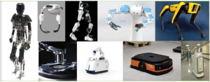
This product is widely used in mobile vehicles, service robots, wearable exoskeleton robots and other products.
Product Series
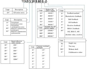
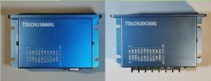
| Model | LDS10B60G | TDLDS15B60G | TDLDS20C60G | LDS40C96 G | LDS65B96G | |||
| Basic Parameters | Rated Current | 10Arms±2% | 15Arms±1% | 20Arms±1% | 40Arms±1% | 65Arms±1% | ||
| Maximum Current | 20Arms±2% | 30Arms±1% | 50Arms±1% | 100Arms±1
% |
130Arms±1% | |||
| Maximum Overload
Time |
30S | 20S | 10S | 6S | 5S | |||
| Overload Recovery
Time |
90S (with external heat dissipation) | |||||||
| Limit Power Supply
Range |
16 VDC~60 VDC | 18 VDC~96VDC | ||||||
| Temperature Rise | Rated current operation 30min≤40K (refer to cooling mode) | |||||||
| Drive Frequency | 6 ~ 21KHz±0.1KHz | |||||||
| Cooling Method | Need auxiliary cooling | Natural cooling | The ventilation condition is good, and the
installation surface needs to have some heat dissipation effect, such as iron plate, steel plate, etc. |
|||||
| Rated Insulation Withstand Voltage | Leakage current of input and output to the chassis DC 1000V is less than 3mA | |||||||
| Insulation Resistance of the Whole
Machine |
When the temperature is 40° and the humidity is 95%, ≥1M (no dew on the board) | |||||||
| Mean Time Between Failures (MTBF) | ≥5000 hours | |||||||
| Power Control Method | Vector control | |||||||
| Protection Level | Remarks:
no shell |
IP32 | ||||||
| Basic Port
Information |
1 Analog Voltage
Input Port |
Analog input 1, 12-bit AD acquisition.
Input impedance: 10KΩ, input analog voltage: -10V~+10VDC |
||||||
| IO Control Input Port | No IO input | 4 IO inputs | 6 IO inputs | |||||
| Voltage input range: 12~24VDC, the software can set the high and low to be effective,
the default input low is effective, and the built-in current-limiting resistor is 4.7K. |
||||||||
| Digital IO Output
Port |
No IO output | 2 IO output | 4 IO output | |||||
| Open collector output, maximum withstand voltage 30V, maximum continuous current
300mA, the software can set the output valid state, the default output is not conductive |
||||||||
| Control Interface of
Position Loop |
No control interface | Compatible with 5V interface, if
compatible with other voltages, external series resistance is required |
Compatible with 5V and 12V~24V interface | |||||
| There are isolated digital signal control and differential pair control. The external IO
input can form two control modes: A/B pulse, direction + pulse, and the highest frequency of digital signal control is 500K |
||||||||
| Brake Control | External power supply is required, with a maximum withstand voltage of 60V and a
maximum output current of 2A. |
|||||||
| Vent Interface | No | Recommended
external 20 Ω 30W |
Recommended
external 10 Ω50W |
Recommended
external 2 Ω 150W |
Recommended
external 1 Ω 200W |
|||
| 1 USB Interface | The interface is a Type-C interface, used for computer software debugging. | |||||||
| 1 485 Interface | The modbus protocol is compatible with ASCII and RTU. | |||||||
| 1 CAN Interface | CANOPEN protocol (Cia DS301 and Cia DSP402), a custom CAN protocol. | |
| Feedback Method | Incremental encoder ABZUVW (differential), ABZ signal can be configured as TTL,
UVW as hall signal |
|
| Basic Functions | Operating Mode | Position loop/speed loop/torque loop control, factory default speed loop control mode |
| Power-on Ready
Time |
No fault after power-on, the drive is ready within 3S | |
| IO Input Configuration (Control Command) | Servo start, position loop pulse error clearance, zero speed clamp, position command
trigger, torque limit, speed limit, speed command, torque command, mode switching command, emergency stop, reverse rotation prohibition limit, forward prohibition limit, positive Jog, reverse jog, return to origin, origin search command, abnormal reset, speed loop gain switch, input reverse command, electronic gear numerator, communication protocol |
|
| IO Output Configuration (Control Command) | Power supply undervoltage, abnormal position, Hall error (abnormal feedback),
overcurrent, overload, EEPROM failure, IGBT failure, drive overheating, motor phase loss, current out of tolerance, speed out of tolerance, motor overheating, power supply overvoltage, servo ready , Servo operation, zero speed arrival, target speed arrival, torque limit, warning, brake output, origin return completion, load threshold exceeded, error alarm, command completion, direction locked rotor, forward locked rotor, reverse indication |
|
| Fault Protection | Power supply undervoltage, abnormal position, Hall error, overcurrent, overload,
EEPROM failure, IGBT failure, driver overheating, motor phase loss, current out-of-tolerance, speed out-of-tolerance, motor overheating, power supply overvoltage, speeding failure, brake opening failure , Encoder error, version error, internal error |
|
| Environmental Requirements | Operating
Temperature |
0℃~+45℃ (no freezing) |
| Storage Temperature | -10℃~+65℃ (no freezing) | |
| Relative Humidity | 5%~90%RH (no condensation) | |
| Height | Below 2000 meters above sea level | |
| Vibration
Requirements |
Frequency: from 5Hz to 25Hz, amplitude 1.6mm, 25Hz to 200Hz, 1.2g, 30min; |
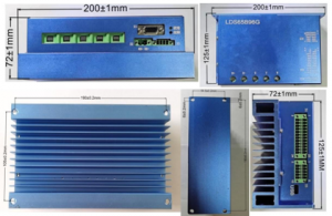
2.Dimensions
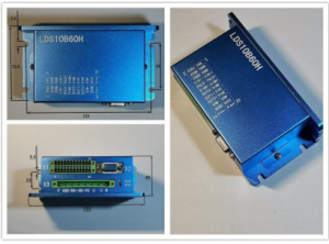
3.Interface Definition
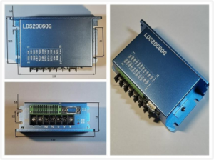
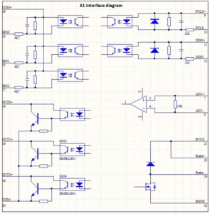
1.X1 Interface Definition of LDS10B60G, LDS15B6G, TDLDS20C60G
| Communication terminal interface definition and wire diameter, terminal, crimping tool selection | |||||
| Pin no. | Signal name | Signal definition | Harness selection | Terminal model | Crimping tool |
| 1 | CANL | CAN bus (without 120 resistance), terminal resistance must be added | It is recommended to use a wire harness with a tinned copper braid with
a copper core wire cross-sectional area of 0.5mm² |
E0506 tube type pre-insulated terminal | HSC86-4 European style terminal special crimping tool |
| 2 | 485A | 485 bus (without 120 resistance) | |||
| 3 | CANH | CAN bus (without 120 resistance), terminal resistance must be added | |||
| 4 | 485B | 485 bus (without 120 resistance) | |||
| 5 | CGND | CAN bus and 485 bus ground, it is recommended to connect to the ground | |||
| 6 | CGND | CAN bus and 485 bus ground, it is recommended to connect to the ground | |||
| 7 | AIN0+ | The analog input main reactance is 10K,
Input voltage range: -10V~10V. |
|||
| 8 | AIN0- | ||||
| 9 | PULS+ | Pulse signal, working voltage is 5V. If you need a higher voltage and need
an external input resistance, please refer to the following direction + pulse interface |
|||
| 10 | PULS- | ||||
| 11 | SIGN+ | Direction signal, working voltage is 5V. If you need a higher voltage and
need an external input resistance, please refer to the following direction +pulse interface |
|||
| 12 | SIGN- | ||||
| 13 | DIN0 | Digital input 0, compatible voltage 12V~24V. | |||
| 14 | DIN3 | Digital output 3, compatible voltage 12V~24V. | |||
| 15 | DIN1 | Digital input 1, compatible voltage 12V~24V. | |||
| 16 | OUT0+ | Digital output 0, open collector output withstand voltage 30V/300mA. | |||
| 17 | DIN2 | Digital input 2, compatible voltage 12V~24V. | |||
| 18 | OUT1+ | Digital output 1, open-collector output withstand voltage 30V, 300mA | |||
| 19 | COM+ | The digital input is a common anode port, and the optocoupler input is a common positive | |||
| 20 | COM- | Digital output common ground port, common ground for optocoupler output | |||
| 21 | BVCC | The brake power supply is positive, and the maximum withstand voltage is 60V. | |||
| 22 | BGND | Brake power supply ground | |||
| 23 | Brake+ | Connect holding brake 2 wires | |||
| 24 | Brake- | ||||
3.2 X1 interface definition of LDS40C96G
| No. | Name | Definition |
| 1 | 485A | 485 BUS (without 120 resistance) |
| 2 | 485A | |
| 3 | 485B | |
| 4 | 485B | |
| 5 | CANL | CAN BUS (without 120 resistance), terminal resistance must be added |
| 6 | CANL | |
| 7 | CANH | |
| 8 | CANH | |
| 9 | CGND | CAN BUS and 485 BUS ground,
it is recommended to connect to the ground |
| 10 | CGND |
3.3 X2 Feedback Definition of LDS10B60G, LDS15B6G, TDLDS20C60G
| Feedback is G series feedback terminal X3 interface definition &
wiring harness selection |
||||
| Pin no. | Signal | Pin no. | Signal | Wiring selection |
| 1 | B+ | 9 | V- | It is recommended to use a wire harness with a tinned copper braid with a copper core wire cross-sectional area of 0.15 mm2 |
| 2 | A+ | 10 | U- | |
| 3 | W+ | 11 | Z+ | |
| 4 | V+ | 12 | Z- | |
| 5 | U+ | 13 | +5V | |
| 6 | B- | 14 | GND | |
| 7 | A- | 15 | PE | |
| 8 | W- | |||
| If it is Hall feedback, you need to communicate with the manufacturer to confirm the
hardware, and connect to U+, V+, W+, +5V, GND. |
||||
3.4 X2 interface definition of LDS40C96G
| Communication terminal interface definition &
wire diameter, terminal, crimping tool selection |
|||||
| Pin
no. |
Signal
name |
Signal definition | Wiring
selection |
Terminal
model |
Crimping
tool |
| 1 | AIN1+ | The analog input main reactance is 10K,
Input voltage range: -10V~10V |
It is recommended to use a wire harness with a tinned copper braid with a copper core wire cross-sectional area of 0.5 mm2 | E0506 Tube type pre- insulated terminal | HSC8 6-4 Crimping tool for EU terminal |
| 2 | AIN1- | ||||
| 3 | PLUS
+ |
Pulse signal, working voltage is 5V. If you need a higher voltage and need
an external input resistance, please refer to the following direction + pulse interface |
|||
| 4 | PLUS- | ||||
| 5 | OPC1 | Refer to 4.4 Figure 3 for pulse signal
input. Compatible with 12V |
|||
| 6 | OPC2 | Refer to 4.4 Figure 3 for pulse signal
input. Compatible with 12V |
|||
| 7 | SIGN+ | Direction signal, working voltage is
5V. If a higher voltage is required and an external input resistance is required, please refer to the direction + pulse interface below. |
|||
| 8 | SIGN- | ||||
| 9 | DIN0 | Digital input 0, 1, 2, compatible
voltage 12V ~ 24V. |
|||
| 10 | DIN1 | ||||
| 11 | DIN2 | ||||
| 12 | OUT0
+ |
Digital output 0, open collector
output withstand voltage 30V, 300mA |
|||
| 13 | DIN3 | Digital input 3, compatible voltage
12V~24V. |
|||
| 14 | OUT1
+ |
Digital output 1, open collector
output withstand voltage 30V, 300mA |
|||
| 15 | DIN4 | Digital input 4, compatible voltage
12V~24V. |
|||
| 16 | OUT2
+ |
Digital output 2, open collector
output withstand voltage 30V, 300mA |
|||
| 17 | DIN5 | Digital input 5, compatible voltage
12V~24V. |
|||
| 18 | OUT3
+ |
Digital output 3, open collector
output withstand voltage 30V, 300mA |
|||
| 19 | COM+ | The digital input is a common anode port, and the optocoupler input is a
common positive |
|||
| 20 | COM- | Digital output common ground port,
common ground for optocoupler |
|||
| output | |||||
| 21 | BVCC | The brake power supply is positive, and the maximum withstand voltage
is 60V. |
|||
| 22 | BGND | Brake power supply ground | |||
| 23 | Brake
+ |
Connect holding brake 2 wires | |||
| 24 | Brake- |
3.5 X3 interface definition of LDS40C96G
| Feedback is G series feedback terminal X3 interface definition &
wiring harness selection |
||||
| Pin no. | Signal | Pin no. | Signal | Wiring selection |
| 1 | B+ | 9 | V- | It is recommended to use a wire harness with a tinned copper braid with a copper core wire cross-sectional area of 0.15 mm2 |
| 2 | A+ | 10 | U- | |
| 3 | W+ | 11 | Z+ | |
| 4 | V+ | 12 | Z- | |
| 5 | U+ | 13 | +5V | |
| 6 | B- | 14 | GND | |
| 7 | A- | 15 | PE | |
| 8 | W- | |||
| If it is Hall feedback, connect to U+, V+, W+, +5V, GND. For single-ended feedback,
connect to signal +. When soldering, the pin serial number and the pin serial number marked on the butt male header can be matched one by one. |
||||
| Feedback is G series feedback terminal X3 interface definition &
wiring harness selection |
||||
| Pin no. | Signal | Pin no. | Signal | Wiring selection |
| 1 | SIN- | 9 | DATA+ | It is recommended to use a wire harness with a tinned copper braid with a copper core wire cross-sectional area of 0.15 mm2 |
| 2 | COS- | 10 | CLOCK+ | |
| 3 | REF- | 11 | SD- | |
| 4 | DATA- | 12 | SD+ | |
| 5 | CLOCK- | 13 | +5V | |
| 6 | SIN+ | 14 | GND | |
| 7 | COS+ | 15 | PE | |
| 8 | REF+ | |||
| SIN, COS, REF are resolver signals, and REF is resolver excitation.
DATA and CLOCK are the feedback signals of SSI and BISS-C, and pins 13 to 15 are used for power supply and shielding. SD is the feedback signal of the 485 absolute encoder, and pins 13 to 15 are used for power supply and shielding. When soldering, the pin serial number and the pin serial number marked on the butt male header can be matched one by one. |
||||
3.6 Power Interface of LDS10B60G, TDLDS15B60G
| No. | Name | Definition | High temperature
wear-resistant multi-strand copper core cross-sectional area |
| 1 | + | Input power “+” | 2~3mm2 |
| 2 | – | Input power “-“ | 2~3mm2 |
| 3 | RB | Bleeding resistance (the other end of the bleeding resistance is
connected to +) |
0.5~2mm2 |
| 4 | PE | Shell shielding ground | 0.5~2mm2 |
| 5 | U | Motor U phase | 2~3mm2 |
| 6 | V | Motor V phase | 2~3mm2 |
| 7 | W | Motor W phase | 2~3mm2 |
3.7 Power Interface of TDLDS20C60G
| No. | Name | Definition | High temperature
wear-resistant multi-strand copper core cross-sectional area |
| 1 | + | Input power “+” | 4.5~6mm2 |
| 2 | – | Input power “-“ | 6mm2 |
| 3 | RB | Bleeding resistance (the other
end of the bleeding resistance is connected to +) |
1.5~3mm2 |
| 4 | PE | Shell shielding ground | 1.5~3mm2 |
| 5 | U | Motor U phase | 64.5~mm2 |
| 6 | V | Motor V phase | 4.5~6mm2 |
| 7 | W | Motor W phase | 4.5~6mm2 |
3.8 Power interface of LDS40C96G
| No. | Name | Definition | High temperature
wear-resistant multi-strand copper core cross-sectional area |
| 1 | + | Input power “+” | 6mm2 |
| 2 | – | Input power “-“ | 6mm2 |
| 3 | RB | Bleeding resistance (the other end of the bleeding resistance is
connected to +) |
3mm2 |
| 4 | PE | Shell shielding ground | 3mm2 |
| 5 | U | Motor U phase | 6mm2 |
| 6 | V | Motor V phase | 6mm2 |
| 7 | W | Motor W phase | 6mm2 |
4 Interface Instructions
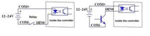
1.Instructions for DIN0~DIN5
- Connect the contacts of switch relays or open-collector output transistors.
- When using contact input, please use a small amount of electricity to prevent poor contact of the switch relay.
- In order to ensure the primary side current of the photocoupler, please keep the lower limit voltage of the power supply (12~24V) above 11.4V.
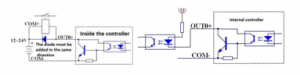
4.2 Instructions for OUT0+~OUT3+
- The output circuit is formed as an open collector output. Connect the relay or photocoupler.
- It is not recommended to connect the output to a TTL IC chip, as it may not be recognized at low level.
- When receiving each output signal through logic circuits such as gates, please be careful not to be affected by noise.
- The recommended current for the primary side of the photocoupler is 10mA.
- The output open-collector transistor has a maximum withstand voltage of 30V and a continuous current of 300mA. It is used to pay attention to the current when the relay is turned on.
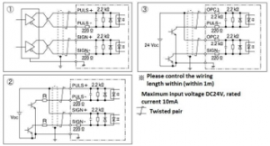
4.3 Direction + Pulse Signal Instructions
① Long-line drive I/F (Maximum allowable input frequency of command pulse input signal: 500Kpps) This is a signal transmission method that is not easily affected by noise. In order to improve the accuracy of signal transmission, this method is recommended.
② Open collector I/F (the maximum allowable input frequency of the command pulse input signal: 200Kpps) is a method that uses the power supply (VDC) for the control signal external to the driver.
In this case, a current limiting resistor corresponding to VDC is required.
Please connect the specified resistance (R). (R) The anti-interference performance is better when it is arranged near the drive.
③ Open collector I/F (Maximum allowable input frequency of command pulse input signal: 200Kpps)
Connection when the current limit resistor is not used in the 24V power supply state.
4.4 Schematic Diagram of Different Wiring Methods of Direction + Pulse Signal
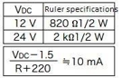
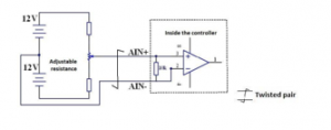
5.Analog Input Description
- The maximum allowable input voltage is ±10V. The input impedance is 10KΩ.
- When using variable resistors (VR) and resistors (R) to form a simple command circuit, please connect as shown in the figure below. When the variable range of each input is -10V~+10V, please set VR to 2 KΩ characteristic 1/2W or more, and R to 200Ω 1/2W or more.
- The resolution of the input AD converter is 12bit.
4.6 Brake Output
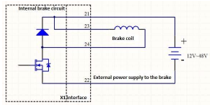
- The maximum output current of the brake is 2.2A, with internal current limiting protection.
- The voltage range of the brake is 12V to 48V, but the voltage needs to be provided externally.
- The brake interface has 21, 22, 23, 24 at the X1 interface.
- The use of the holding brake requires the host computer to be turned on, and the delay time for opening and closing must
be configured. If the brake circuit is turned on, it will detect whether the external brake circuit will be disconnected.
7.Bleeder Circuit
- The bleeder resistors of LDS10B60G and TDLDS15B60G are connected to RB+ and RB-. The recommended bleeder
resistor is 10 ohm 30W.
- The bleeder resistor of TDLDS20C60G is connected to + and RB. The recommended bleeder resistor is 10 ohm 50W.
- The bleeder circuit can be turned on in the upper computer configuration. If the software is not configured, the bleeder
circuit is turned on by default at 70V, and the hysteresis voltage is 3V.
5.Communication
1.Rs485 Communication
The figure below is the schematic diagram of Rs485 communication wiring.
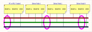
The communication line of Rs485 communication should not be run together with high-voltage line or high-current power line. For the precautions of wiring, please refer to 4.2 Communication Cable Wiring Mode below.
5.2 CAN Communication
The figure below is a schematic diagram of CAN communication wiring.
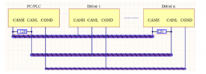
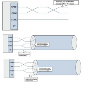
- It is recommended to use shielded twisted pair connection, and two 120Ω terminal matching resistors are connected to both ends of the bus to prevent signal reflection.
- Use a multimeter to measure the resistance between CANL and CANH to confirm whether the field termination
resistance is correct. The normal resistance value should be about 60Ω. (Two resistors in parallel)
- The maximum number of connected devices is 64.
- When CAN devices communicate over long distances, the common ground GND of different CAN circuits must be connected to each other to ensure that the reference potentials between different communication devices are equal.
- Do not run CAN communication lines with high-voltage lines or high-current power lines.
The following figure shows the introduction of twisted pair cable for CAN communication
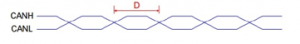
- The twisted pair torque D should be less than 2cm, the smaller the torque, the better the anti-interference.
- In short-distance and low-speed communication, twisted-pair shielded cables can be used to increase the anti- interference ability, and the shielding layer can be double-terminated with PE.
- For long-distance high-speed communication, it is not recommended to use shielded cables. Because of the large
distributed capacitance between the shielding layer and the signal line, the transmission signal will be delayed.
5.3 Different Wiring Methods of Communication Cables
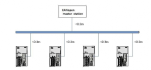
If you use the topological interface in the figure above, pay attention that the length of each branch is less than 0.3m. Whether it will cause reflections and cause communication problems.
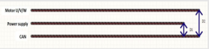
The interference line and the CAN line should be routed vertically as far as possible. When the line is routed in parallel, the distance between the power supply and the CAN signal line is D1>10cm, and the distance between the motor U/V/W and the CAN signal D2>15cm.
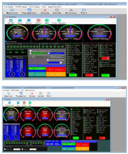
- Debugging software
Revision history
| Version | Date | Reason |
| V0.90 | 2018/03/27 | Create a document; |
| V0.91 | 2019/08/01 | Modify some text and pictures; |
Disclaimer
This document provides instructions for using related products. This document does not grant any intellectual property license, and does not grant any intellectual property license either expressly or implicitly, or by prohibiting speech or other means. In addition, we do not make any express or implied warranty for the sale and/or use of this product, including the suitability of the product for a specific purpose, marketability, or liability for infringement of any patent rights, copyrights or other intellectual property rights. This drive is an industrial-grade product and is not designed for medical, life-saving or life-saving purposes. We may make changes to product specifications and product descriptions at any time without notice.